
PCBWay Manufacturing Review
PCBs are a fundamental part of our day-to-day in modern life, forming part of the devices that surround us. From professionals to makers or hackers, being able to manufacture our own PCBs is fundamental for innovation and the creation of new products.
Thanks to the great accessibility that exists today to manufacture professional-grade PCBs for less than the cost of materials for home manufacturing, it makes home-etch boards or other types of diy boards less and less necessary. This also favors the complexity of developments, ensuring high quality and reducing costs by eliminating possible manufacturing failures.
Factories that specialize in making small to medium sized batches are very popular for making PCBs in a short time frame, for less than a dollar a unit for the most common manufacturing options. One such factory is PCBWay, which is the subject of this review.
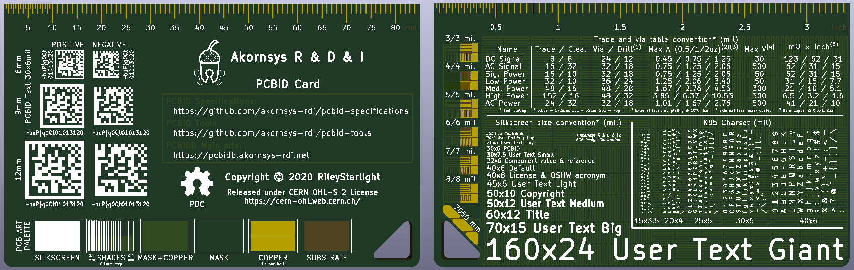
In order to prepare the review, the PCBID Card PCB has been used, of which 10 units have been manufactured. You can see the design of this board in this repository. This board has no electronic functionality, but it is a card with useful information. This board has the following characteristics.
- Ruler: Two-sided 85 mm (3.346 inch) ruler, with a scale in millimeters and inches, with a resolution of half a millimeter and 25 thousand.
- URL: URL links to relevant PCBID web addresses.
- 2D Barcode: PCBID table in datamatrix and text format with samples at different sizes in positive and negative.
- PCB Art Palette: Palette of layers of PCB materials.
- Lanyard hole: Side hole in the card to insert a lanyard.
- Trace width sample: Layouts of traces with different trace and clearance sizes.
- Trace and via table: Table that crosses the current capacity, maximum voltage and resistance with the size of traces and via for usual types of layouts.
- Silkscreen size: Sample of different silkscreen sizes, with their common uses.
- K85 Charset: The character set of K85 at different screen sizes to check its readability.
- Maze layout: Provides a background with horizontal and vertical traces to simulate the readability of silkscreen on a conventional PCB. The trace that draws this layout has a width of 250µm and a length of 7050mm.
This board has not been designed specifically for this review, but because of some of its features it is excellent for this purpose. Among the boards manufactured, one has been chosen at random for analysis. It is important to say that this board does not have any drills, so this aspect cannot be evaluated.
Ordering
PCBID Card is designed with KiCad 5. For its manufacture, the gerbers of the necessary layers have been generated and zipped (in this case copper, mask and silkscreen layers for both sides plus board outline, no drill file is generated).
PCBWay offers many manufacturing options through its website. Some of them are advanced and difficult to find in other manufacturers, making it one of the manufacturers with more product offerings. A complete list can be seen on the online quote form. The whole ordering process is simple and friendly, guided step by step.
The review board PCBID Card is manufactured with the following options:
- Quantity: 10
- Size: 54 × 85 mm
- Layers: 2 layers
- Material: FR-4 TG 130/140
- Thickness: 1.6 mm
- Minimum Track/Spacing: 6/6
- Minimum Hole Size: No drill
- Solder Mask: Green
- Silkscreen: White
- Surface Finish: HASL with lead
- Finished Copper: 1 oz
With these manufacturing options, the boards cost $5. When the gerber file is uploaded, an automatic check is made to ensure that everything is correct. It takes four working days from the time the order is completed online to the time it is shipped from the factory. It is fair to say that the manufacturing of these boards was held back because the drill file was missing. Once this matter has been clarified with the technical service, manufacturing is resumed.
Shipping time and packaging
Shipping of the boards costs $7 using the E-packet shipping method. With this type of shipping it is estimated that the delivery time will be between 30 and 35 calendar days, in exchange for being the most economical. The package takes 27 calendar days to arrive, considering that it is in the context of the global Covid-19 pandemic.
The package consists of a cardboard box with the PCBWay logo well taped, containing between bubble wrap fillings a gift sticker and the vacuum packed bubble wrap boards with desiccant. When the packaging is opened, 13 boards appear (10 were ordered) perfectly stacked. Vacuum packing is important, because it prevents the boards from moving freely during the shipping time and from causing damage by rubbing or shock.
Board inspection
Result of the visual and with tools of measurement analysis of the board PCBID Card. The results obtained are compared with the capabilities table of PCBWay and evaluated according to the experience of different manufacturers.
Dimensions
The dimensions of the board in design are 54 × 85 × 1.6 mm. According to the caliper, the dimensions of the board under analysis are 54.1 × 85.2 × 1.6 mm. The board also has a triangular cut inside, being this cut 0.1 mm larger than the design.
The rulers that PCBID Card has coincide perfectly with a professional ruler, both for the millimeter and the inch scale.
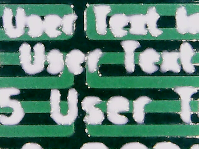
Silkscreen
All text and logos on the silkscreen layer are clearly distinguishable. The height of the silkscreen layer is uniform on both sides of the board. PCBWay recommends a minimum of 0.15 mm in the thickness of the silkscreen, which is infringed by the board under analysis in different occasions. The lines of 0.1 mm are well defined. All six 2D barcodes are read without problems.
PCBID Card> contains texts in silkscreen from 15 × 3.5 mil onwards, being almost half of the minimum recommended by PCBWay (32 × 6 mil are the minimum measures recommended for correct text recognition). The texts are quite well distinguished and readable, even those out of specification can be read with the help of a magnifier or microscope.
Solder mask
The solder mask is bright, uniform and well applied, does not peel or scratch easily. It shows no traces of contamination or halos. The distance between mask and exposed copper is correct and equidistant on all edges. It is not possible to know how it is deposited on vias as it does not have this kind of drill.
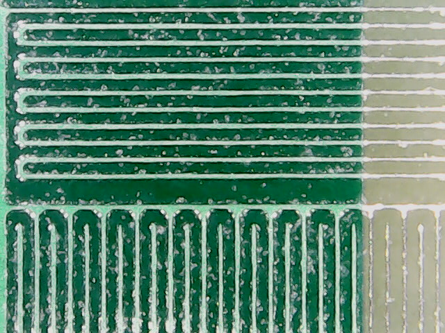
Copper
It is important to remember that the board is manufactured under the minimum track/spacing option of 6/6 mil. PCBID Card contains a sample of zig-zag traces of different sizes, from 8 to 3 mils in 1 mil steps. This zig-zag composes two circuits, one open and one closed between two pads, for each trace size. Both in optical and multimeter inspection, all traces including the 3/3 mil are without defect, which speaks very well of the machinery available in the factory.
The traces have the correct width. The chosen HASL finish is applied with a uniform thickness on both large and small areas.
The thickness of copper is difficult to measure, so a resistive system is used to check it. It takes advantage of a feature that has the board PCBID Card which is the maze layout. Knowing the length of a trace, its thickness and width, and knowing the resistivity of copper per unit distance, you can calculate how much resistance that track should have. In this case the trace is 7050 mm long, 250 µm wide and 35 µm high, resulting in a theoretical resistance of 13.89 Ω. The measurement reveals a resistance of 13.86 Ω. With a difference of 27 mΩ, it can be concluded that it is really 35 µm of copper, and that the measurements of the track are accurate.
Technical support
When you create your account on the PCBWay website you are automatically assigned a technical support person who speaks your selected preferred language. The technical support is friendly and close, giving a quick response. If a problem is encountered they will write to you immediately to discuss the issue.
Summary
When you see the finished boards, you get the feeling that they have been processed with high precision machinery, giving a high quality finish. A proof of this is that they have been able to be successfully traced at 3/3 mil with 6/6 mil technology. It is also surprising how many manufacturing options they have.
As if the service they offer were not enough, PCBWay is committed to students and makers, providing discounts, a large community of developers with referrals and a web platform for open-source projects.
Among the PCB manufacturers I have worked with, PCBWay is not the cheapest of them (not counting shipping), but still there is no doubt that their prices are very competitive ($5 !!) and the quality provided is very high.
We at Akornsys R & D & I intend to continue manufacturing our projects with PCBWay. Create your account and use this link to get a discount on your first order.